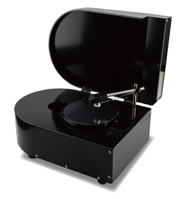
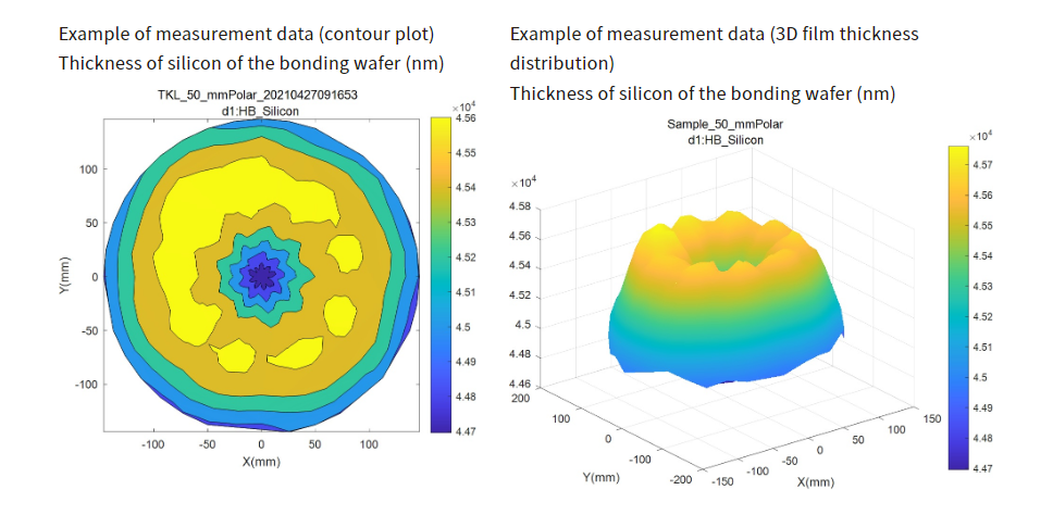
The wafer mapping unit is capable of automatic mapping film thickness measurement over the entire surface of wafers up to 300 mm. The automatic alignment function, self-calibration function and high flatness wafer chuck enable highly reliable film thickness measurement. This unit is used in combination with the compact film thickness monitor.
It can be installed at the load port of semiconductor manufacturing equipment to control the film thickness on the manufacturing equipment while maintaining cleanliness.
Automatic film thickness mapping measurement of up to 300 mm wafer is possible.
Automatic alignment function.
Automatic calibration function.
Improved measurement reliability in the wafer surface by adopting a wafer chuck with high flatness.