Singapore
SG
China
CN
Malaysia
MY
Indonesia
ID
Myanmar
MM
Products
Laboratory Essentials
Analytical Science
Life Science
Material Science & Nanotechnology
Pharmaceuticals
Brands
Services
Webinar
Contact Us
Home
About Us
Careers
Promotions
News & Events
Our Network
+603 8065 3889
/
+603 8065 3989
/
info@gaiascience.com.my
Material Science & Nanotechnology
Home
Products
Material Science & Nanotechnology
Material Characterisation
Thin Film Measurement
Non-contact Sheet Resistance Mapping EddyCus TF Map 2525
Back
Thin Film Measurement
Non-contact Sheet Resistance Mapping EddyCus TF Map 2525
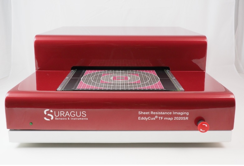
The EddyCus TF map 2525SR automatically measures the sheet resistance of large samples up to 250 x 250 mm² (10 x 10 inches) in non-contact mode
Pricing & Availability
Download Catalogue
Brand:
Suragus
Quick Share:
Contact Us
for better pricing.
Warranty Details

Overview
Specification
Downloads
Product Images
Product Videos
Product Enquiry
Advantages
Non-contact real time measurement of substrates up to 250 x 250 m² (10 x 10 inches)
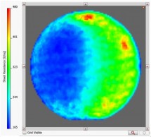
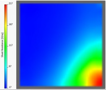
High resolution mapping of conductive thin films
Characterization even of hidden and encapsulated conductive layers
Various software-integrated analysis functions (e.g. sheet resistance distribution, line scans, single point analysis)
Measurement data saving and export functions
Measurement characteristics
Sheet resistance
Thin layer uniformity control
Defect detection and coating analysis
Measurement and mapping of metal layer thickness
Quality control, input and output control
Sample sizes: 50 x 50 mm² to 250 x 250 mm² (2 x 2 inches to 10 x 10 inches)
Measurement range: 0.001 to 1,000 Ohm/sq
Applications
Coated architectural glass, e.g. LowE
Displays, touch screens and flat panel displays
OLED and LED applications
Smart glass
Graphene layers
Photovoltaic wafers and cells
Semiconductor wafers
Metallization layers and wafer metallization
De-icing and heating applications
Battery electrodes
Conductively coated paper and conductive textiles
Software and device control
Very user-friendly software
Real-time mapping measurement
Easy-to-use statistical analysis options
Various data analysis, data saving and export options
Specification :
Measurement technology
Non-contact eddy current sensor
Substrates
e.g. foil, glass, wafer
Max. scanning area
10 inch / 254 x 254 mm (larger on request)
Edge effect correction / exclusion
2 mm edge exclusion for standard sizes
Max. sample thickness/ sensor gap
2 / 5 / 10 / 25 mm (defined by the thickest sample/ application)
Sheet resistance range and accuracy
0.0001 – 10 Ohm/sq < 2% accuracy
10 – 100 Ohm/sq < 3% accuracy
100 – 1,000 Ohm/sq < 5% accuracy
Thickness mapping of metal films (e.g. Aluminum, Copper)
2 nm – 2 mm (in accordance with sheet resistance)
Scanning pitch
1 / 2 / 5 / 10 mm (other on request)
Measurement points per time (quadratic shape)
10.000 measurement points in 5 minutes
1.000.000 measurement points in 30 minutes
Scanning time
4 inch / 200 x 200 mm in 0.5 to 5 minutes (1 – 10 mm pitch)
8 inch / 200 x 200 mm in 1.5 to 15 minutes (1 – 10 mm pitch)
Device dimension (w/h/d) / Weight
23.6 x 9.05 x 31.5 inch / 600 x 230 x 800 mm / 27 kg
Available features
Metal thickness imaging
Anisotropy sheet resistance sensor
Optical transmission sensors at 632 nm wavelength
GSM_Suragus_EdduCusTF2525_Catalogue1.pdf
*
Name :
*
Company :
*
Phone Number :
*
Email :
*
Product :
Additional Remarks :
Submit
Reset
Back to product list
Previous Product
Next Product
×
Warranty Details
Product Warranty :
1 year against manufacturing defects
×
Email
*
Name of Recipient :
*
E-mail of Recipient :
*
Your Name :
*
Your E-mail address :
*
Personal message :
Submit
Reset
×
Sign In Here
Sign In to Start Your Session
I Forgot My Password
Sign In
×
Main Menu
Products
Laboratory Essentials
Analytical Science
Life Science
Material Science & Nanotechnology
Pharmaceuticals
Quick Links
Home
Products
About Us
Brands
Careers
Services
Webinar
Contact Us
Promotions
News & Events
Our Network
Customer Service
Enquiry
Help & FAQ
Terms and Conditions